- 您现在的位置:买卖IC网 > Sheet目录3884 > PIC17C766T-33E/PT (Microchip Technology)IC MCU CMOS 33MHZ 16K EPRM80TQFP
Section 4 Clock Pulse Generator (CPG)
Page 90 of 1336
R01UH0025EJ0300 Rev. 3.00
Sep 24, 2010
SH7261 Group
4.4.2
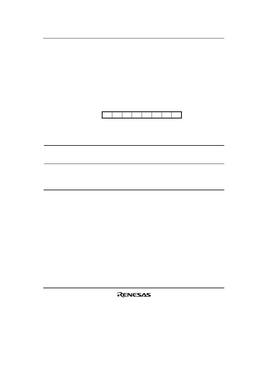
CKIO Control Register (CKIOCR)
CKIOCR is an 8-bit readable/writable register used to control output of the CKIO pin. When this
LSI is started in clock operating mode 3, writing 1 to this register is invalid.
When this LSI is started in clock operating mode 3, CKIOCR is initialized to H'00 by a power-on
reset caused by the
RES pin or in deep standby mode. When this LSI is started in clock operating
mode 0 or 2, CKIOCR is initialized to H'01 by a power-on reset caused by the
RES pin or in deep
standby mode. This register is not initialized by an internal reset triggered by an overflow of the
WDT, a manual reset, in sleep mode, or in software standby mode.
7654321
0
0/1*
R
0
R
0
R
0
R
0
R
0
R
0
RR/W
Bit:
Initial value:
R/W:
———
—
——
—
CKIO
OE
Bit
Bit Name
Initial
Value
R/W
Description
7 to 1
All 0
R
Reserved
These bits are always read as 0. The write value
should always be 0.
0
CKIOOE
0/1*
R/W
CKIO Output Enable
Enables output of the CKIO pin.
0: Output from CKIO is not enabled.
1: Output from CKIO is enabled.
Note:
*
The initial value depends on the clock operating mode of the LSI.
发布紧急采购,3分钟左右您将得到回复。
相关PDF资料
PIC17C766T-33E/L
IC MCU CMOS 33MHZ 16K EPRM84PLCC
PIC17C766T-16E/PT
IC MCU CMOS 16MHZ 16K EPRM80TQFP
PIC17C766T-16E/L
IC MCU CMOS 16MHZ 16K EPRM84PLCC
PIC17C766-33E/PT
IC MCU CMOS 33MHZ 16K EPRM80TQFP
PIC17C766-33E/L
IC MCU CMOS 33MHZ 16K EPRM84PLCC
PIC16C54C-20/P
IC MCU OTP 512X12 18DIP
PIC17C766-16E/PT
IC MCU CMOS 16MHZ 16K EPRM80TQFP
PIC17C766-16E/L
IC MCU CMOS 16MHZ 16K EPRM84PLCC
相关代理商/技术参数
PIC17C766T-33I/L
功能描述:8位微控制器 -MCU 33MHz 16K EPRM RoHS:否 制造商:Silicon Labs 核心:8051 处理器系列:C8051F39x 数据总线宽度:8 bit 最大时钟频率:50 MHz 程序存储器大小:16 KB 数据 RAM 大小:1 KB 片上 ADC:Yes 工作电源电压:1.8 V to 3.6 V 工作温度范围:- 40 C to + 105 C 封装 / 箱体:QFN-20 安装风格:SMD/SMT
PIC17C766T-33I/PT
功能描述:8位微控制器 -MCU 32KB 902 RAM 66 I/O RoHS:否 制造商:Silicon Labs 核心:8051 处理器系列:C8051F39x 数据总线宽度:8 bit 最大时钟频率:50 MHz 程序存储器大小:16 KB 数据 RAM 大小:1 KB 片上 ADC:Yes 工作电源电压:1.8 V to 3.6 V 工作温度范围:- 40 C to + 105 C 封装 / 箱体:QFN-20 安装风格:SMD/SMT
PIC17LC42A-08/L
功能描述:8位微控制器 -MCU 4KB 232 RAM 33 I/O RoHS:否 制造商:Silicon Labs 核心:8051 处理器系列:C8051F39x 数据总线宽度:8 bit 最大时钟频率:50 MHz 程序存储器大小:16 KB 数据 RAM 大小:1 KB 片上 ADC:Yes 工作电源电压:1.8 V to 3.6 V 工作温度范围:- 40 C to + 105 C 封装 / 箱体:QFN-20 安装风格:SMD/SMT
PIC17LC42A-08/P
功能描述:8位微控制器 -MCU 4KB 232 RAM 33 I/O RoHS:否 制造商:Silicon Labs 核心:8051 处理器系列:C8051F39x 数据总线宽度:8 bit 最大时钟频率:50 MHz 程序存储器大小:16 KB 数据 RAM 大小:1 KB 片上 ADC:Yes 工作电源电压:1.8 V to 3.6 V 工作温度范围:- 40 C to + 105 C 封装 / 箱体:QFN-20 安装风格:SMD/SMT
PIC17LC42A-08/PQ
功能描述:8位微控制器 -MCU 4KB 232 RAM 33 I/O RoHS:否 制造商:Silicon Labs 核心:8051 处理器系列:C8051F39x 数据总线宽度:8 bit 最大时钟频率:50 MHz 程序存储器大小:16 KB 数据 RAM 大小:1 KB 片上 ADC:Yes 工作电源电压:1.8 V to 3.6 V 工作温度范围:- 40 C to + 105 C 封装 / 箱体:QFN-20 安装风格:SMD/SMT
PIC17LC42A-08/PT
功能描述:8位微控制器 -MCU 4KB 232 RAM 33 I/O RoHS:否 制造商:Silicon Labs 核心:8051 处理器系列:C8051F39x 数据总线宽度:8 bit 最大时钟频率:50 MHz 程序存储器大小:16 KB 数据 RAM 大小:1 KB 片上 ADC:Yes 工作电源电压:1.8 V to 3.6 V 工作温度范围:- 40 C to + 105 C 封装 / 箱体:QFN-20 安装风格:SMD/SMT
PIC17LC42A-08I/L
功能描述:8位微控制器 -MCU 4KB 232 RAM 33 I/O RoHS:否 制造商:Silicon Labs 核心:8051 处理器系列:C8051F39x 数据总线宽度:8 bit 最大时钟频率:50 MHz 程序存储器大小:16 KB 数据 RAM 大小:1 KB 片上 ADC:Yes 工作电源电压:1.8 V to 3.6 V 工作温度范围:- 40 C to + 105 C 封装 / 箱体:QFN-20 安装风格:SMD/SMT
PIC17LC42A-08I/P
功能描述:8位微控制器 -MCU 4KB 232 RAM 33 I/O RoHS:否 制造商:Silicon Labs 核心:8051 处理器系列:C8051F39x 数据总线宽度:8 bit 最大时钟频率:50 MHz 程序存储器大小:16 KB 数据 RAM 大小:1 KB 片上 ADC:Yes 工作电源电压:1.8 V to 3.6 V 工作温度范围:- 40 C to + 105 C 封装 / 箱体:QFN-20 安装风格:SMD/SMT